[ad_1]
Superior TC NCF expertise enhances vertical density and thermal properties
Samsung positioned to fulfill demand for high-performance and high-capacity options within the AI period

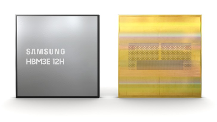
Samsung Electronics, a world chief in superior reminiscence expertise, at this time introduced that it has developed HBM3E 12H, the {industry}’s first 12-stack HBM3E DRAM and the highest-capacity HBM product to this point.
Samsung’s HBM3E 12H supplies an all-time excessive bandwidth of as much as 1,280 gigabytes per second (GB/s) and an industry-leading capability of 36 gigabytes (GB). Compared to the 8-stack HBM3 8H, each facets have improved by greater than 50%.
“The {industry}’s AI service suppliers are more and more requiring HBM with greater capability, and our new HBM3E 12H product has been designed to reply that want,” mentioned Yongcheol Bae, Govt Vice President of Reminiscence Product Planning at Samsung Electronics. “This new reminiscence answer kinds a part of our drive towards creating core applied sciences for high-stack HBM and offering technological management for the high-capacity HBM market within the AI period.”
The HBM3E 12H applies superior thermal compression non-conductive movie (TC NCF), permitting the 12-layer merchandise to have the identical top specification as 8-layer ones to fulfill present HBM bundle necessities. The expertise is anticipated to have added advantages particularly with greater stacks because the {industry} seeks to mitigate chip die warping that include thinner die. Samsung has continued to decrease the thickness of its NCF materials and achieved the {industry}’s smallest hole between chips at seven micrometers (µm), whereas additionally eliminating voids between layers. These efforts lead to enhanced vertical density by over 20% in comparison with its HBM3 8H product.
Samsung’s superior TC NCF additionally improves thermal properties of the HBM by enabling using bumps in varied sizes between the chips. Through the chip bonding course of, smaller bumps are utilized in areas for signaling and bigger ones are positioned in spots that require warmth dissipation. This technique additionally helps with greater product yield.
As AI functions develop exponentially, the HBM3E 12H is predicted to be an optimum answer for future methods that require extra reminiscence. Its greater efficiency and capability will particularly permit clients to handle their assets extra flexibly and scale back complete price of possession (TCO) for datacenters. When utilized in AI functions, it’s estimated that, compared to adopting HBM3 8H, the typical velocity for AI coaching will be elevated by 34% whereas the variety of simultaneous customers of inference companies will be expanded greater than 11.5 instances.1
Samsung has begun sampling its HBM3E 12H to clients and mass manufacturing is slated for the primary half of this 12 months.
1 Based mostly on inner simulation outcomes
[ad_2]
Source link
